Semiconductor wafer price manufacturers
I have found results from600+products and300+suppliers aboutSemiconductor wafer price
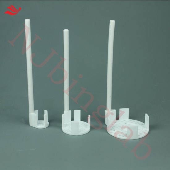
Laboratory Semiconductor Wafer Storage PTFE Wafer Cassette, 4-Inch, 6-Slot, with Handle
Semiconductor Laboratory PTFE Wafer Cassette for Single-Wafer 4/7cm Cleaning, Customizable Sizes
PTFE Wafer Cassettes for Storing Semiconductor Wafers, 100/150/200mm, Are Customizable
Single Wafer Carrier PTFE Dipper Transporting Wafer for Semiconductor Processing
4-Inch PTFE Wafer Carrier Suitable for Wafer Etching During Semiconductor Manufacturing Process
Semiconductor PTFE Dippers Wafer Cleaning Size Can Be Customized for a Variety of Wafers
8" Hf PFA Resistant Semiconductor Silicon Wafer Carrier
Semiconductor Laboratory PTFE Wafer Cassette 5cm Silicon Wafer Immersion Cleaning
PFA Wafer Cassette Resistant to HCl Hf Semiconductor Clean
PTFE Wafer Cassette Can Be Customized Semiconductor Silicon Wafer Cleaning Tank
5-Inch Translucent PFA Semiconductor Cleaning Silicon Wafer Box with Strong Acid and Alkali Resistance
Si Wafer Silicon Plate Si Substrate Optical Silicon Wafer Semiconductor Wafers
Sapphire Wafer Al2O3 Single Crystal Semiconductor Substrate Customizable Diameter High Transparency Optical Grade Silicon Wafer
Semiconductor Silicon Wafer Semi-Conductor Silicon Plate Infrared Thermometer Filter Wafers
Patterned Silicon Wafer/Bare Silicon Wafer for Semiconductor Manufacturing
0.35 mm N-Type Conductive Epitaxial Silicon Carbide Sic Semiconductor Wafer
Semiconductor Grade N-Type/P-Type Silicon Wafer (Custom Thickness)
P-Type Silicon Wafers Monocrystalline Silicon Wafer Best Price for Semiconductor
4-8 Inch Diameter Semiconductor Substrate Silicon Carbide (SiC) Wafer
Premium Silicon Wafer Blanks for Semiconductor Manufacturing Applications
High Temperature Jgs1 /Jgs2 Quartz Glass Plate Transparent Quartz Semiconductor Wafer
Semiconductor Device Fabrication Fab Wafer Fab Rie Reactive Ion Etching Failure Analysis Equipment Beol Feol
Compound Semiconductor SLC LED Mems Wafer Fabrication Fab Rtp Rapid Thermal Processing Equipment
Semiconductor Testing Equipment Wafer Measurement Analysis / Wafer Manual Prober
Semiconductor Substrate Materials Wafer Dicing Equipment / Lab Manual Scribe and Break System / Manual Wafer Scriber
Semiconductor Fab Wafer Flattening Removing Nanoscale Planarization Chemical Mechanical Planarization CMP Process
Fab Wafer Fabrication Rapid Thermal Processing Desktop Rtp System for Compound Semiconductors
Semiconductor Device University Wafer Lab Fab Equipment Reactive Ion Etching Rie System
Customized Sic Silicon Carbide Ceramic Semiconductor Wafer
G1 Wafers/M6 Wafers/Semiconductor Wafers/Monocrystalline Silicon Wafers
Silicon Wafer/Optical Silicon Wafer/Semiconductor Silicon Wafer/Silicon Chips
Silicon Wafer/Silicon Plate/Silicon Slice/Optical Silicon Wafer/Semiconductor Silicon Wafer
Optical Grade Silicon Wafer / Semiconductor Si Wafer for Laser Infrared Optical Components
Premium Custom Silicon Wafers for Advanced Semiconductor Manufacturing
Semiconductor Material 6h Sic Wafer Single Crystal (Silicon Carbide) Silicon Wafer
Semi-Automatic Sintalke Stk-5020 Wafer Detaper High-Precision Semiconductor Wafer Detaping
Automatic Semiconductor Equipment Supplier Nitto Rhsa840II Wafer Detaping
Automatic Nitto Hr8500III Semiconductor Equipment Wafer Detaping
Automatic Nitto Hsa840 Semiconductor Equipment Wafer Detaping
Sintalke Stk-5150 Semiconductor Equipment Supplier Thinner Wafer Detaping
Cheap Nitto Hr3000III Semiconductor Equipment Supplier Automatic Wafer Detaping
Semiconductor 8inch 200mm Silicon Thermal Oxide Wafer
300mm Silicon Polished Wafer Semiconductor Dummy Wafer Monocrystalline Silicon Wafer
Wholesale Customized P-Type N-Type Semiconductor 12 Inch Silicon Wafer Best Price for Semiconductor Silicon Wafer
4inch Silicon Polished Wafer Semiconductor Test Dummy Wafer
Japanese Quality Semiconductor Substrate CZ 8 Inch P Type Test Dummy Film Silicon Wafer
Chinese IC Supplier Monocrystalline Silicon Semiconductor Wafer Price
China Supplier Zhendi Manufacturer SCR Semiconductor Soi Wafer
China Supplier Zhendi Manufacturer SCR Thyristor Semiconductor Wafer Price Silicon Wafer 100 Price
China Supplier Zhendi Manufacturer Thyristor Semiconductor P/N-Type Wafer
China Supplier Zhendi Manufatcurer Semiconductor Silicon Wafer Chip for Thyristor Appliacation
Polished Round Ceramic Silicon Carbide Sic Semiconductor Wafer
High Thermal Conductivity Aluminum Nitride Ceramic Wafer for Semiconductor
Polished Yttria Stabilized Ysz Zro2 Zirconia Zirconium Oxide Ceramic Semiconductor Wafer
Precision Aln Aluminum Nitride Ceramic Wafer for Semiconductors
Ceramic 96 99.6% Alumina Thin Aluminum Oxide Wafer for Semiconductors
China High-Precision Tel P-8 Probe Station Machine Semiconductor Manufacturing Equipment Wafer Prober
High-Reliability Used Tel P-8 Probe Station Machine Semiconductor Manufacturing Equipment Wafer Prober
China Used Tel P-12XL Probe Station Machine Semiconductor Manufacturing Equipment Wafer Prober
China High-Consistency High-Yield Tel P-12XL Probe Station Semiconductor Manufacturing Machine Wafer Prober
China Automatic Used Tel P-8 Probe Station Semiconductor Manufacturing Equipment Wafer Prober
High Purity Monocrystalline Silicon Wafer N Type P Type Polished Si Wafer for Semiconductor Mems Research Solar Device
6-Inch Silicon Wafer/Silicon Wafer/Wafer/Semiconductor Wafer
8-Inch Silicon Wafer/Silicon Wafer/Wafer/Semiconductor Wafer
12-Inch Silicon Wafer - Ideal for Cutting-Edge Semiconductor Technology
Premium 12-Inch Silicon Wafer for Advanced Semiconductor Applications
IC Wafer Edge Chamfering Equipment for Semiconductor Fab
Semiconductor Wafer Chamfering Equipment for IC Manufacturing
Silicon Wafer Edge Profiling Equipment for Semiconductor Wafer
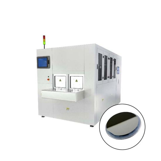
Semiconductor Wafer Double Side Lapping Equipment
Semiconductor Silicon Wafer Double Side Grinding Equipment
Alumina Ceramic Wafer End Effectors for Semiconductor Wafer
Silicon Carbide / Alumina Porous Ceramic Wafer for Semiconductor Vacuum Chuck
Semiconductor Used Customized Mirror Polish Aluminum Nitride Plate Ain Ceramic Disc Wafer
High Thermal Conductivity Aluminum Nitride Ceramic Wafer for Semiconductor
Semi Grade DSP/Ssp<100><111> 2/4/6/8inches Silicon Wafer Si Wafers for Semiconductor
Yutai China Manufacturer 2"/4"/6"/8"/12" Ssp/DSP 100/110/111 N/P-Type Silicon Wafers Si-Wafer for Semiconductor
Semiconductors Single Crystal and Silicon Wafer Made in China
N P Type Semiconductor Silicon Wafer
Likesmile Semiconductor Wafer Thinning Equipment Exporter China
Likesmile Semiconductor Wafer Grinding System for Microelectronics
Likesmile Silicon Wafer Chamfering Machine for Semiconductor Production Line
Likesmile IC Silicon Wafer Chamfering Machine Factory Price
Sourcing guidance for Semiconductor Wafer Price
What are the key technical specifications to consider when evaluating semiconductor wafer quality?
When sourcing semiconductor wafers, you must prioritize substrate material (e.g., Monocrystalline Silicon, SiC, or GaN) and wafer diameter (typically 200mm/8-inch or 300mm/12-inch). Key performance indicators include Total Thickness Variation (TTV), which should be <10μm for high-precision applications, and Surface Roughness (Ra), often required to be <0.5nm. Additionally, verify the doping type (P-type or N-type) and resistivity range to ensure compatibility with your specific integrated circuit (IC) or discrete device design.
How do compliance standards affect the procurement of semiconductor wafers?
Compliance is critical in the electronics supply chain. Ensure suppliers adhere to SEMI Standards, which govern the physical dimensions and safety of semiconductor manufacturing. For environmental and market access, products must be RoHS and REACH compliant to ensure they are free from hazardous substances. Furthermore, sourcing from manufacturers with ISO 9001 (Quality Management) and IATF 16949 (Automotive Quality) certifications is essential if the wafers are intended for automotive or industrial-grade electronics.
What factors influence the economic feasibility and pricing of semiconductor wafers?
The price of semiconductor wafers is highly sensitive to yield rates and grade. Prime Grade wafers are the most expensive due to their near-perfect crystal structure, while Test or Dummy Grade wafers offer a cost-effective solution for equipment calibration. Volume-based pricing is standard; bulk orders exceeding 1,000 pieces can often secure discounts of 10-20%. You should also account for the cleanroom packaging costs, as wafers must be shipped in specialized FOUPs or coin-roll shippers to prevent contamination.
What are the typical usage scenarios for different wafer types?
Usage depends on the bandgap and thermal properties. Silicon (Si) wafers are the standard for consumer electronics like CPUs and memory. Silicon Carbide (SiC) and Gallium Nitride (GaN) are 'Wide Bandgap' semiconductors, ideal for high-power applications such as electric vehicle (EV) inverters and 5G base stations. For optoelectronics like LEDs, Sapphire or GaAs substrates are the primary choice.
Cross-Border Procurement Risks and Strategic Advice
How can I mitigate transaction risks when purchasing high-value semiconductor components?
To ensure transaction security, always use Trade Assurance services provided by reputable platforms like Made-in-China.com. This protects your payment until the goods are verified. For high-value shipments, it is mandatory to hire a third-party inspection agency (such as SGS or Intertek) to perform a Pre-Shipment Inspection (PSI) in a cleanroom environment to verify particle counts and surface defects before the final balance is paid.
What are the logistics and packaging precautions for international shipping?
Semiconductor wafers are extremely fragile and sensitive to static and contamination. Ensure the supplier uses Vacuum-sealed ESD (Electrostatic Discharge) bags and shock-absorbent outer packaging. For international transit, specify Air Freight over sea freight to minimize vibration exposure and humidity risks. Ensure the shipment is labeled with 'Fragile' and 'Sensitive Electronics' indicators, and always secure Full Cargo Insurance covering the total invoice value.
How do international trade policies and export controls impact wafer sourcing?
The semiconductor industry is subject to strict Export Control Classifications (ECCN). Before finalizing a purchase, verify if the specific wafer technology (especially for advanced nodes below 14nm or specialized materials like GaN) requires an Export License from the origin country. Failure to align with International Trade Policies can lead to customs seizures or legal penalties. Consult with a customs broker to confirm the correct HS Code (typically 3818.00) and applicable tariffs in your region.
What strategies should be used for negotiating with semiconductor suppliers?
Focus on Long-term Supply Agreements (LTA) rather than one-off spot purchases. Given the cyclical nature of the semiconductor market, an LTA can guarantee price stability and capacity allocation during shortages. Negotiate for Technical Support and 'Failure Analysis' reports as part of the after-sales package. On platforms like Made-in-China.com, look for 'Diamond Members' or 'Audited Suppliers' to ensure you are dealing with established factories rather than small-scale traders.